This is a demo store. No orders will be fulfilled.
Chemicals solutions in the semiconductor industry
Product Manager
Sandra Forbes

At present, with the rapid development of science and technology, semiconductor materials have become a shining pearl in the field of science and technology, widely penetrating into all aspects of our lives. From smartphones that are frequently used in daily life, to computers that run various complex programs, to cars with powerful functions, semiconductor materials play a crucial role.
With the rapid rise of emerging technologies such as artificial intelligence AI, 5G, and the Internet of Things, the market's requirements for the performance of semiconductor materials are becoming increasingly stringent. As an important supporting force in the semiconductor industry, chemical reagents are deeply involved in and strongly promote the development of the industry from the initial stage of wafer preparation to the final stage of device manufacturing, which in turn profoundly affects our lives.
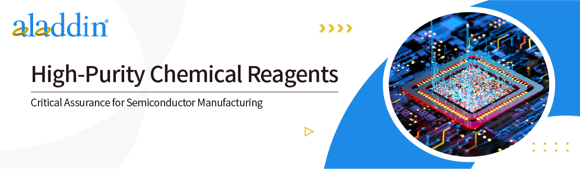
In the development process of semiconductor materials, the purity of chemical reagents has always been a core element, occupying an irreplaceable key position. From wafer cleaning, lithography, etching, doping, thin film deposition, metallization to packaging and testing, every process step cannot be separated from the powerful guarantee of high-purity chemical reagents. High-purity chemical reagents can not only effectively remove impurities and reduce defects, but also significantly improve the yield and performance of devices, which is the key to ensuring the stability and consistency of semiconductor manufacturing processes.
Thin film deposition
In the complete process of semiconductor material manufacturing, the thin film deposition step involves generating various types of thin films with specific functions on the wafer surface, such as insulating layers, conductive layers, and doped layers. The quality of these thin films will directly affect the performance and reliability of semiconductor devices.
The role of chemical purity cannot be ignored during the film deposition process. Even the smallest impurities are likely to cause defects in the film, which will further adversely affect the performance of the device.
Chemical vapor deposition CVD is a commonly used method in the field of thin film deposition. Its principle is to form a solid film on the surface of a wafer by decomposing or participating in chemical reactions with gaseous precursors under high temperature conditions.
Physical vapor deposition (PVD) is a method of achieving thin film deposition on the surface of a wafer through a physical change process. Aladdin Scientific provides high-purity metal elements such as gold (Au), silver (Ag), aluminum (Al), titanium (Ti), tungsten (W), etc., which have significant characteristics such as diverse morphology, high purity, and stable quality. They can effectively reduce the risk of contamination of thin films, improve film quality, and thus help improve device performance.

Photolithography
As a key technology in the semiconductor manufacturing process, lithography plays an important role in accurately defining and transferring tiny patterns onto the wafer surface. It uses light, masks, photoresists and other materials and equipment to transfer the circuit pattern onto the semiconductor material without any deviation, which is one of the core processes in chip manufacturing.
In the lithography process, a uniform layer of photoresist is first applied to the wafer surface, followed by exposure treatment. After the exposure is completed, the photoresist is developed using tetramethylammonium hydroxide TMAH. TMAH has unique chemical properties that can effectively dissolve the exposed parts of positive photoresist, allowing them to detach from the wafer surface, thereby allowing the pre-designed circuit patterns to be clearly visible.
It can be seen that the purity of TMAH has a direct and critical impact on the quality and resolution of the development process. High-purity TMAH can ensure the uniformity and consistency of the development process, effectively avoiding problems such as uneven development and pattern distortion caused by the mixing of impurities, thereby ensuring stable performance and reliable quality of the final manufactured chips.
Etching
Etching processes play a key role in semiconductor manufacturing processes, with their core function being to remove excess material and create specific patterns and structures. The process can be mainly divided into two categories: dry etching and wet etching, and each method has its own unique application scenarios and advantages. Dry etching is particularly good at manufacturing high-precision and high aspect ratio patterns due to its excellent precision control capabilities; Wet etching is characterized by high selectivity and relatively simple process flow.
In the wet etching process, the chemical reagents used, such as hydrofluoric acid, nitric acid, phosphoric acid, hydrochloric acid, sulfuric acid, and potassium hydroxide, play a decisive role in the effectiveness and safety of the etching process. Only by accurately selecting the appropriate etching method and chemical reagent, and continuously optimizing the etching process parameters, can high-quality etching results be achieved, thereby fully meeting the stringent requirements of semiconductor device manufacturing.
The high-purity acid and alkali products provided by the Aladdin brand have significant advantages such as high purity and stable quality. The packaging specifications are flexible and diverse, ranging from grams to tons, and can fully meet the reagent needs of customers from the research and development stage to the production stage. For detailed information on specific product levels and application areas, please refer to the official website of Aladdin Reagents.
Ion implantation
Ion implantation technology is a core technology in the field of semiconductor manufacturing. Its basic principle is to precisely inject specific types of ions into a wafer, thereby changing the electronic properties of the material and shaping the necessary structure for semiconductor devices. In this delicate and critical process flow, the purity of the ion source plays a decisive role in the performance and reliability of semiconductor materials.
In the semiconductor doping process, common doping ions include boron B, phosphorus P, arsenic As, gallium Ga, and indium In. When these ions are introduced into the lattice structure of silicon, they will cause changes in the electronic states of the lattice, which will significantly affect the conductivity properties of silicon, ultimately achieving the goal of adjusting the characteristics of semiconductor devices.
In the process of ion implantation, indium chloride plays an important role as a dopant source, which is widely used in the field of n-type doping, optoelectronic devices and high-frequency electronic devices. The purity level of indium chloride has a crucial impact on the accuracy of the doping process and the performance of the final device. Using high-purity indium chloride as a doping source can effectively reduce the introduction of impurities during the doping process, greatly improve the uniformity of doping, thereby optimizing the overall performance of the material, enhancing the reliability of the device, and simultaneously enhancing the control accuracy and stability of the process.
Clean
In the semiconductor manufacturing process, the cleaning process is the core link to ensure the performance and reliability of the device. The core objective of the cleaning process is to remove organic, inorganic, particulate, and metallic impurities from the surface of silicon wafers and other semiconductor materials, resulting in a clean and flawless surface. This ensures the smooth progress of subsequent processes and guarantees high-quality devices.
In view of this, the choice of chemical reagents is particularly critical, and its importance is self-evident. The quality of chemical reagents directly affects the cleanliness of the wafer surface and the uniformity of etching, which in turn has a significant impact on the performance and yield of semiconductor devices.
Aladdin provides electronic-grade and semiconductor-grade organic solvents and acid/base products with significant advantages of high purity and strong batch stability. These high-quality chemical reagents can effectively improve the cleaning effect, help improve the quality and performance of semiconductor devices, and also lay a solid foundation for high-yield, low-cost production models.
Detection
In the field of semiconductor manufacturing, precise control and strict monitoring of material purity and composition are the core elements to ensure product quality and performance. ICP technologies such as inductively coupled plasma mass spectrometry (ICP-MS) and inductively coupled plasma optical emission spectrometry (ICP-OES) have been widely used in material testing and analysis in the semiconductor industry due to their high sensitivity and accuracy.
Aladdin's PrimorTrace™ trace analysis grade high purity acid exhibits ultra-high purity characteristics and effectively controls the content of 65 metal impurities. The product is packaged in a clean workshop, effectively avoiding the risk of contamination from external sources. When applied to ICP-MS and ICP-OES analysis, it can significantly improve the sensitivity and accuracy of elemental analysis.
Aladdin has always upheld its responsibility to provide high-quality products and unswervingly pursued purity and high-purity standards. With a wide range of chemical products, excellent purity and stable quality, it can fully meet the chemical needs of customers from the research and development stage to the production process, effectively promoting the continuous development and progress of semiconductor materials, and injecting strong impetus into the development of future technologies.
For more semiconductor-related chemicals, please visit the Aladdin Reagent official website: https://www.aladdinsci.com
Aladdinsci: https://www.aladdinsci.com
Categories: Technical articles